Congratulations on the Successful Development of PCBWay's 24-Layer, 6-Order Arbitrary Interconnection HDI PCB
As the integrated circuit industry continues to evolve, the complexity of chip connections has significantly increased. Traditional PCB technology is now struggling to meet the demands of high-frequency and high-speed applications. Ensuring stable and reliable interconnections between high-speed, high-density chips has become a crucial challenge in modern electronics.
Additionally, with the growing power consumption of chips, heat generation has also become a major concern. This necessitates the development of efficient cooling systems to ensure optimal performance and prevent overheating.
In response to these challenges, a new type of PCB called the interposer PCB has emerged as a promising solution.
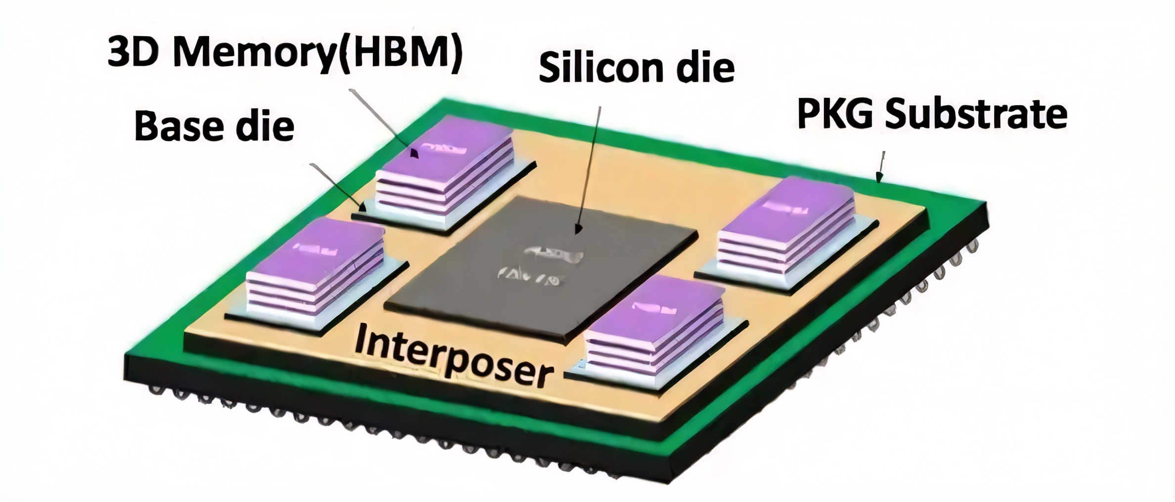
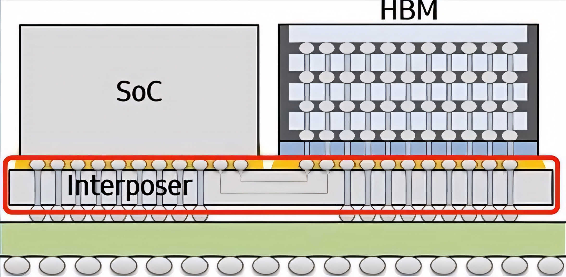
The interposer PCB is a highly advanced, multi-layer HDI (High-Density Interconnect) board that enables precise and complex interconnections between different electronic components. It acts as an intermediary layer between chips, facilitating electrical connections through pad leads and connecting with the chip’s micro bumps (uBump) and internal routing. The interposer uses through-silicon vias (TSV) to link upper and lower layers, enabling high-performance communication between chips.
The design of interposer PCBs includes inner layers connected to outer layers via laser microvias and dense routing, creating a multi-layer structure with BGA (Ball Grid Array) connections on the top and pad connections on the bottom.
Interposer PCBs play a vital role in enhancing the performance of integrated circuits. They offer faster and more reliable connections, improve signal integrity, manage thermal performance, and enable integration of heterogeneous chips, making them essential for next-generation electronics.
First, interposer PCBs provide higher connection speeds and reliability. Using high-performance materials, they support short-distance, high-density connections between chips, significantly increasing data transmission rates.
Second, they help reduce signal loss by minimizing the length of signal paths, improving signal integrity and reducing power consumption.
Third, the interposer layer also contributes to thermal management, helping to dissipate heat and maintain stable chip operation.
Finally, interposer PCBs allow for seamless integration of different types of chips, enhancing system performance and efficiency in applications such as AI, high-performance computing, and data centers.
In conclusion, interposer PCBs are widely used in fields like high-performance computing, artificial intelligence, data centers, and communications. They enable multi-chip integration, boost processing power, and support high-speed data transfer, meeting the growing demand for advanced electronic systems.
As a leading manufacturer of high-end HDI PCBs, PCBWay continuously innovates to meet evolving market needs. In response to the rising demand for high-order arbitrary interconnection (Anylayer) HDI boards, our research team has successfully developed high-layer, high-order interposer PCBs, overcoming complex technical challenges along the way.
Here, we showcase the details of this high-precision circuit product using a 24-layer, 6-order Anylayer HDI PCB as an example.
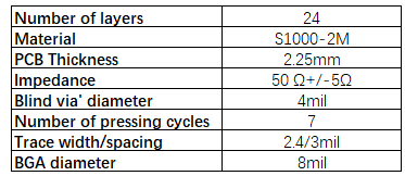
1. Product Parameters
2. Product Structure
3. Technical Challenges
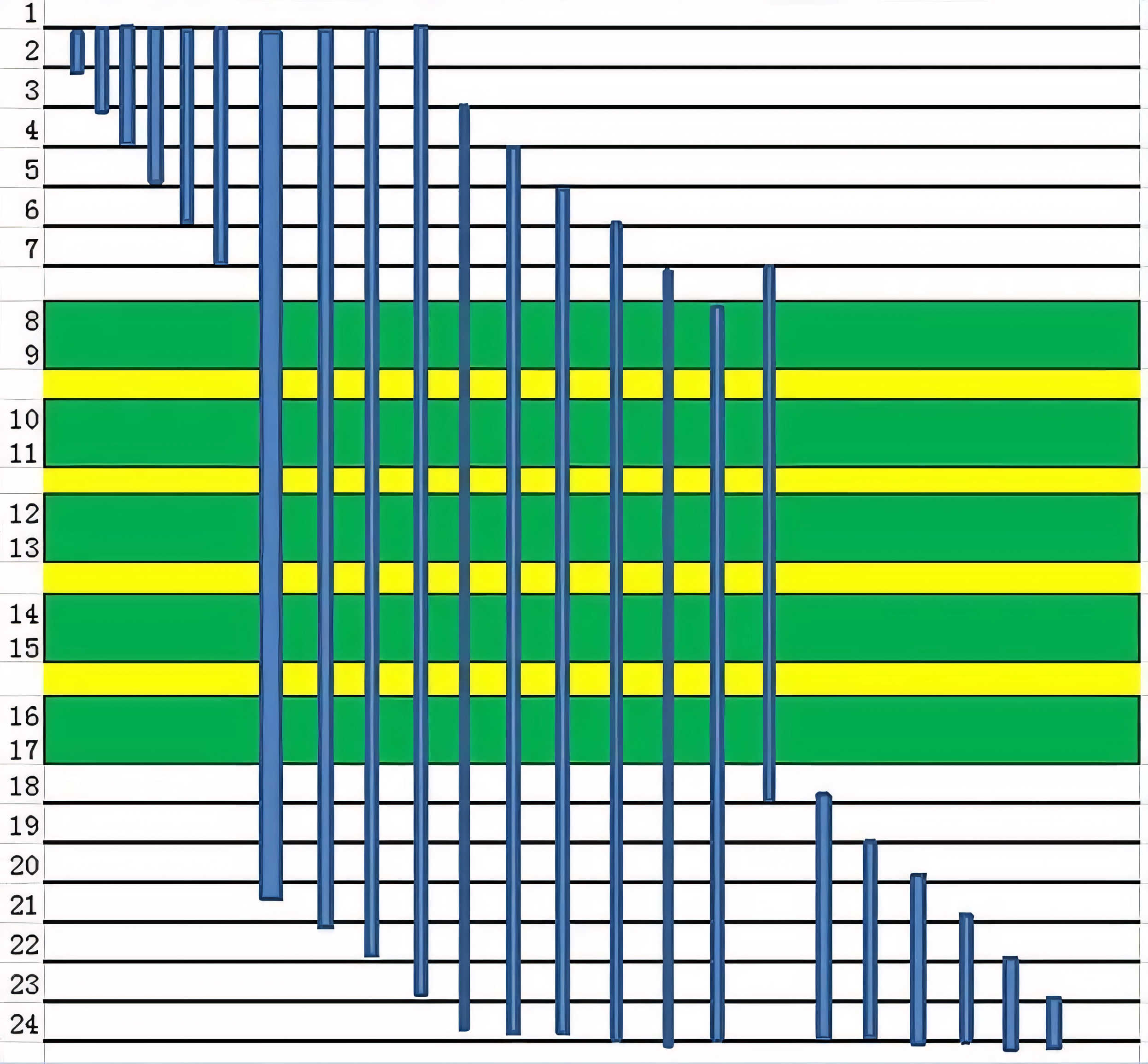
Challenge 1: The buried via thickness from layer 7 to 18 is 1.0 mm, with a mechanical via diameter of 0.1 mm, resulting in a 10:1 aspect ratio, which makes drilling extremely challenging.
Challenge 2: The BGA pitch is 0.35 mm, and the distance from the via to the trace is only 0.13 mm, increasing the risk of misalignment during multiple laminations.
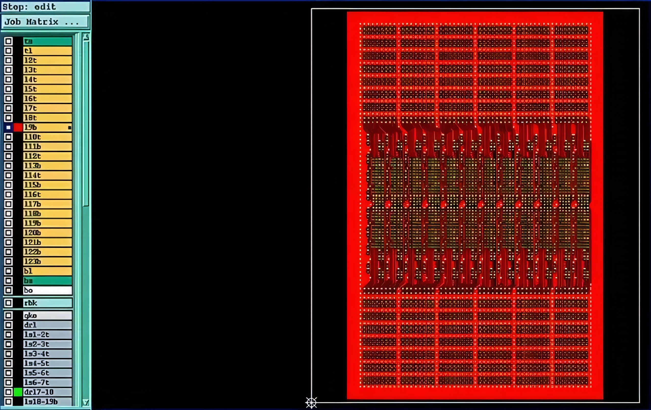
Challenge 3: The trace width and spacing are 2.4 mil and 3 mil respectively, with very dense routing. Below are some examples of the routing layout.
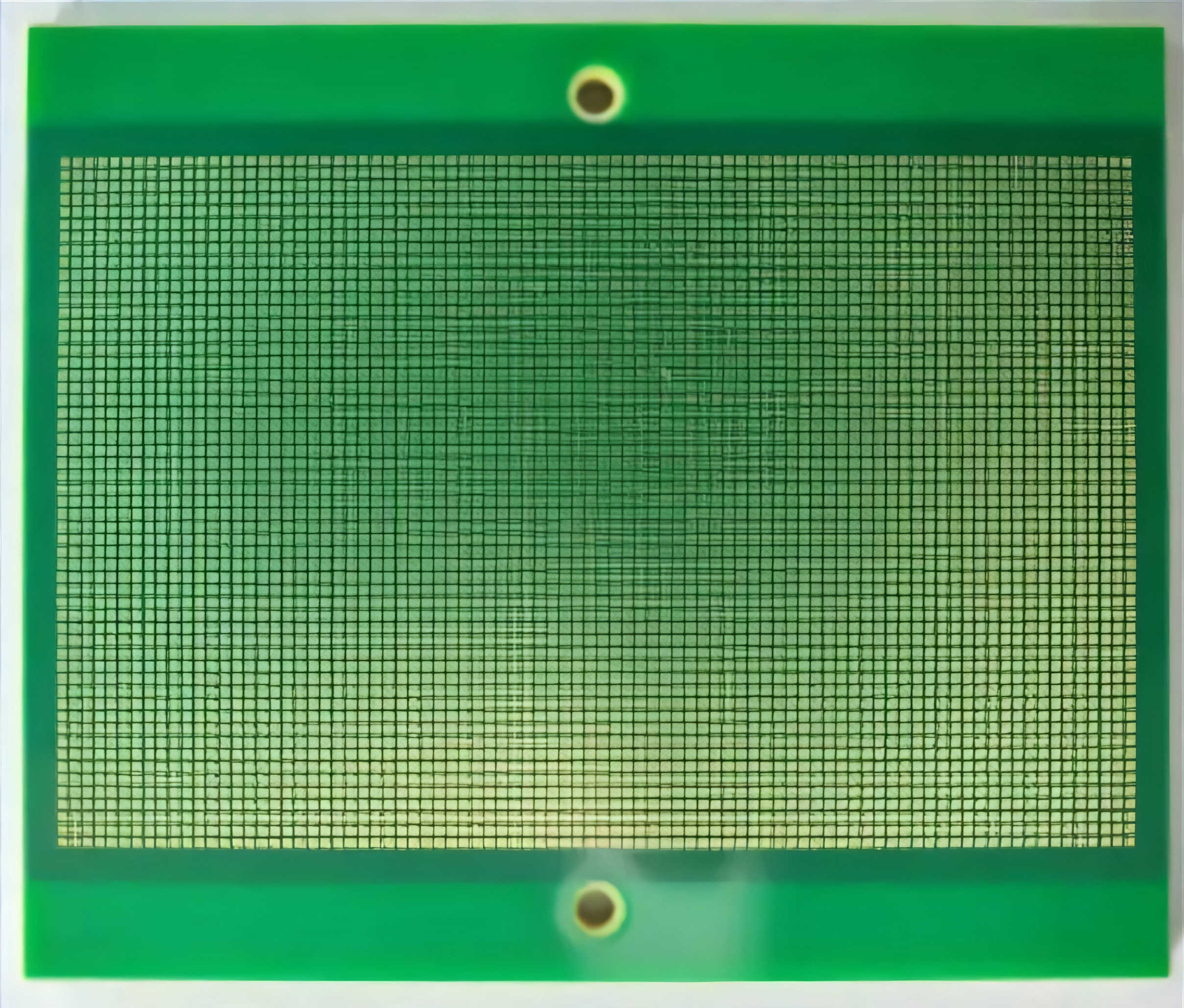
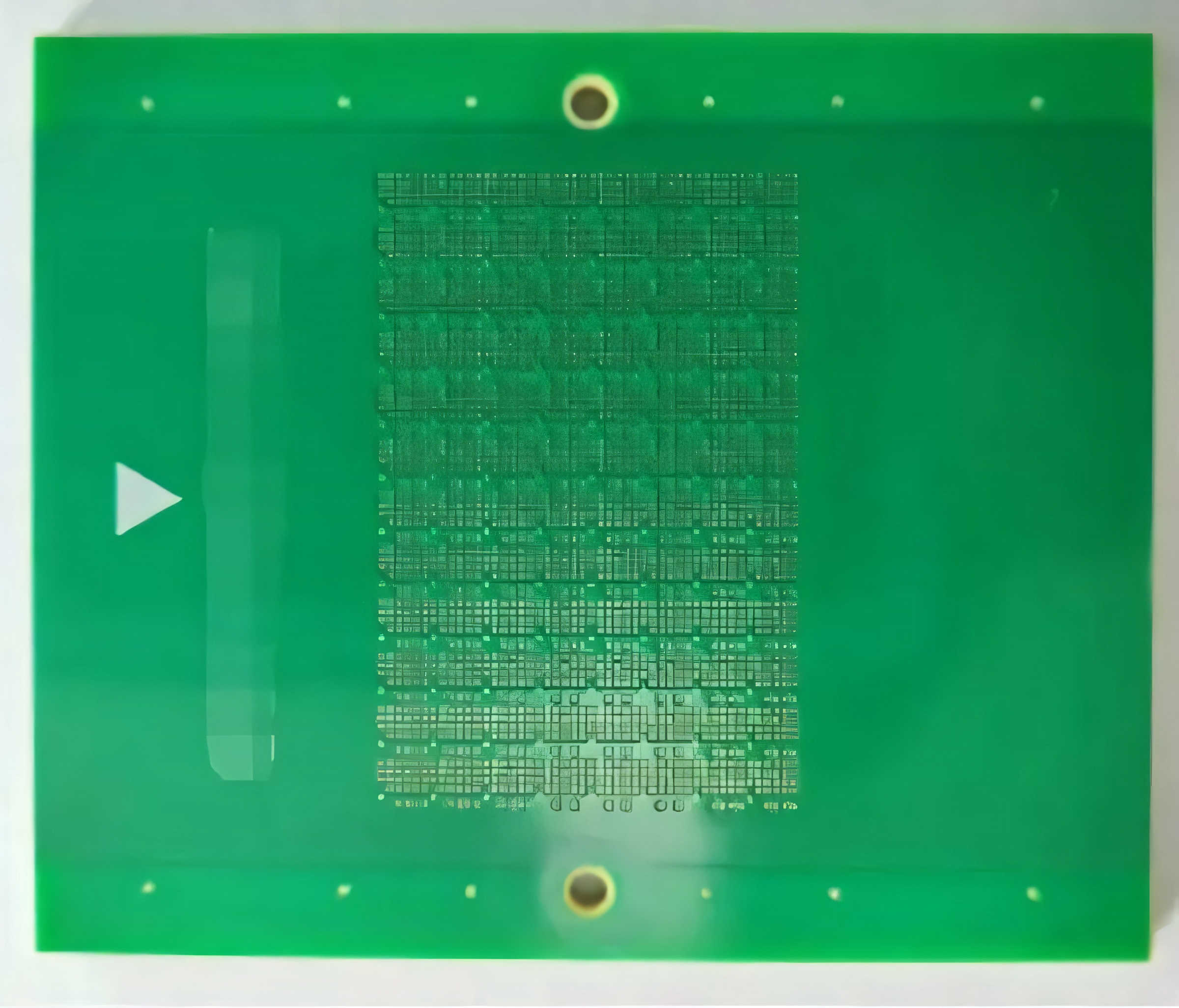
4. Finished Product Images
Heating Products,Candy Floss Machine Cart,Waffle Baker Machine,Automatic Popcorn Machine
JIANGMEN PRO-TAYLOR REFRIGERATION CO., LTD. , https://www.protaylor.com